Pictures

A finished wafer using the previous mask set.
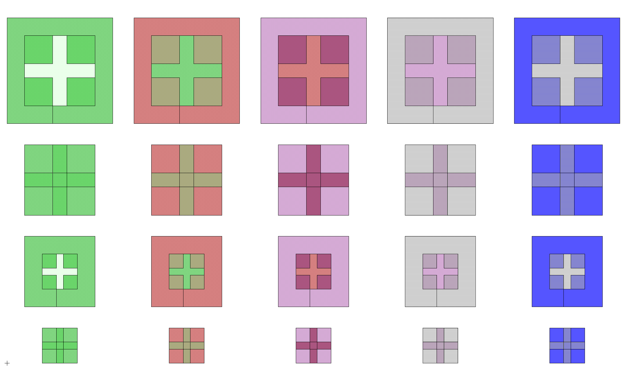
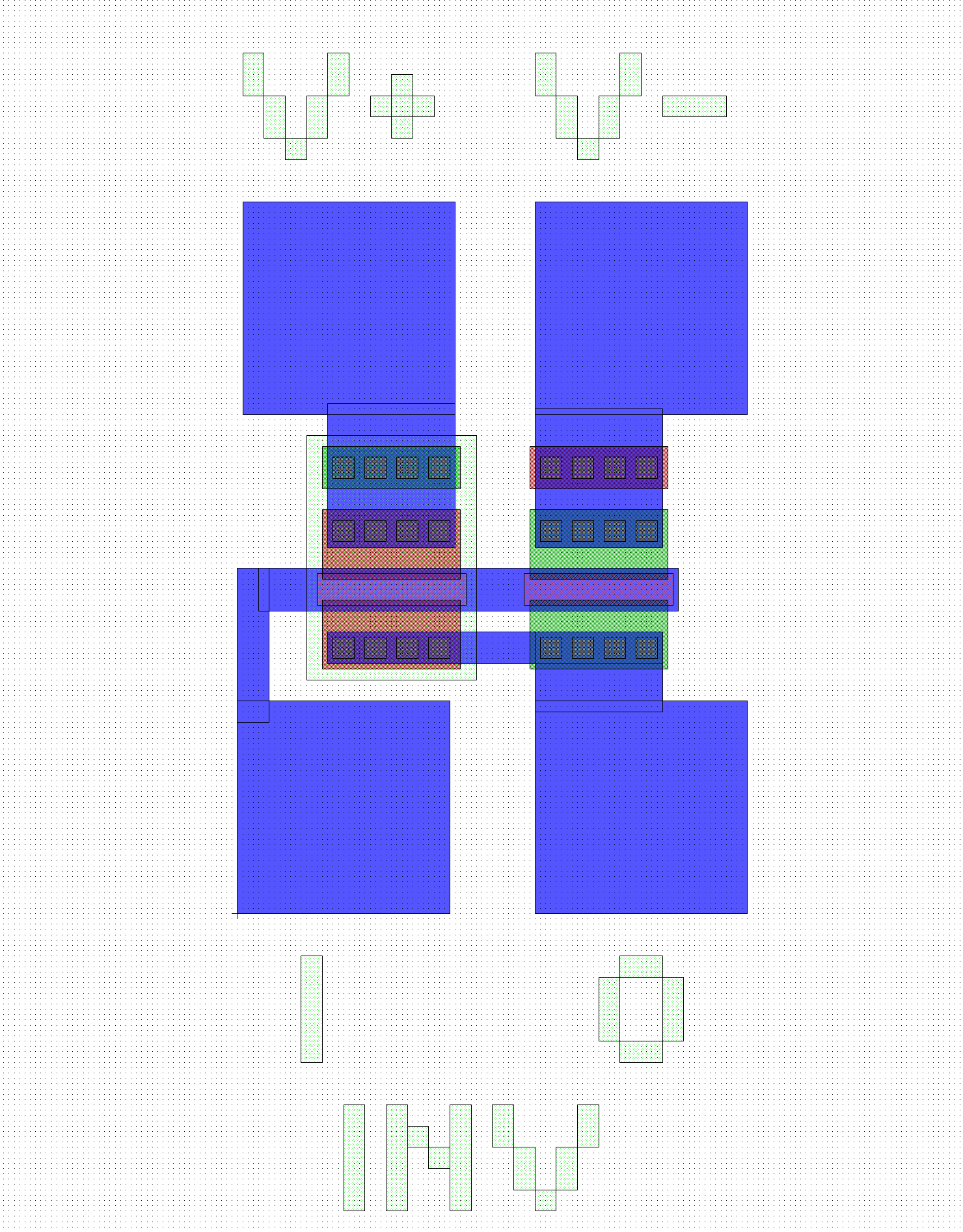
Wafer Layout
Alignment marks.
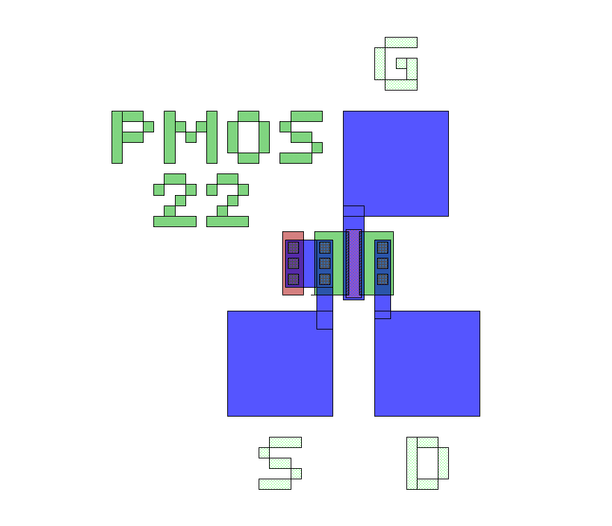
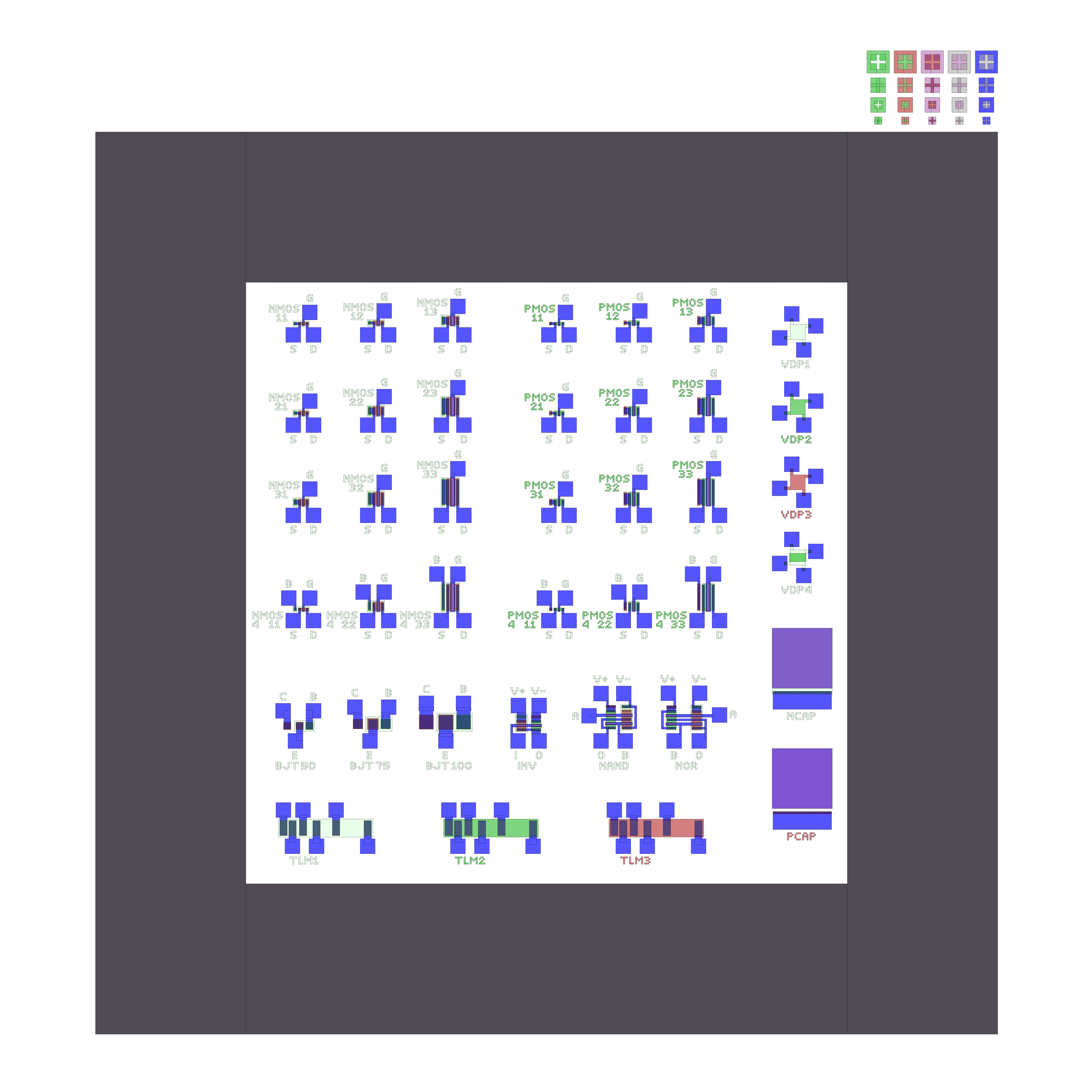
Layout of 3-terminal PMOS
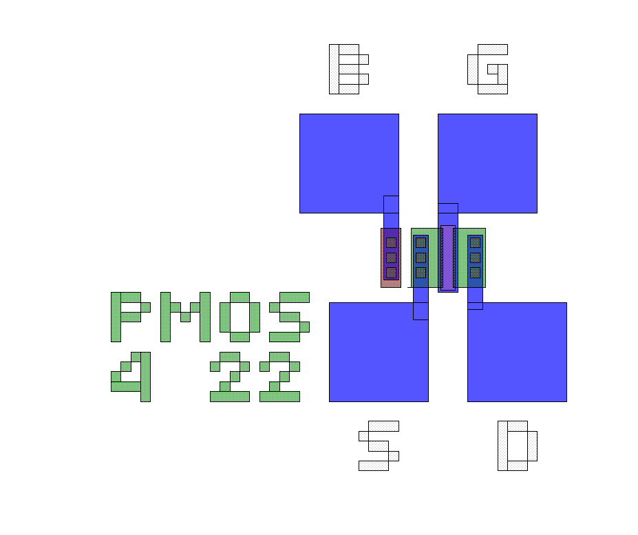
Layout of 4-terminal PMOS
Layout of 3-terminal NMOS
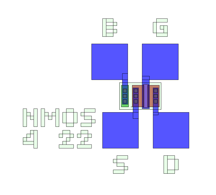
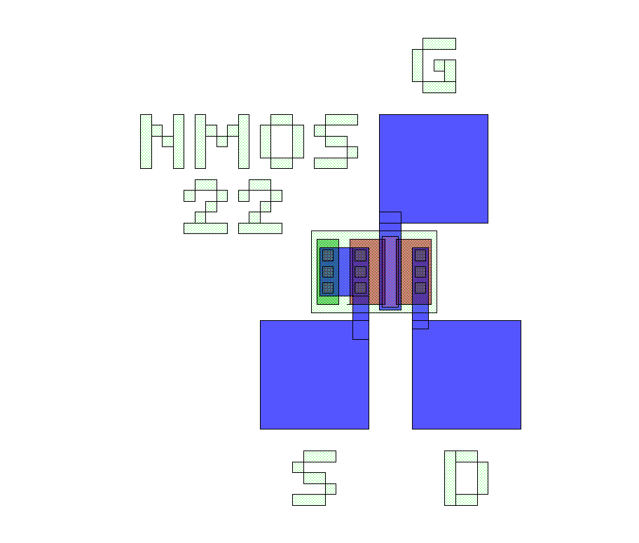
Layout of 4-terminal NMOS
Layout of an Inverter
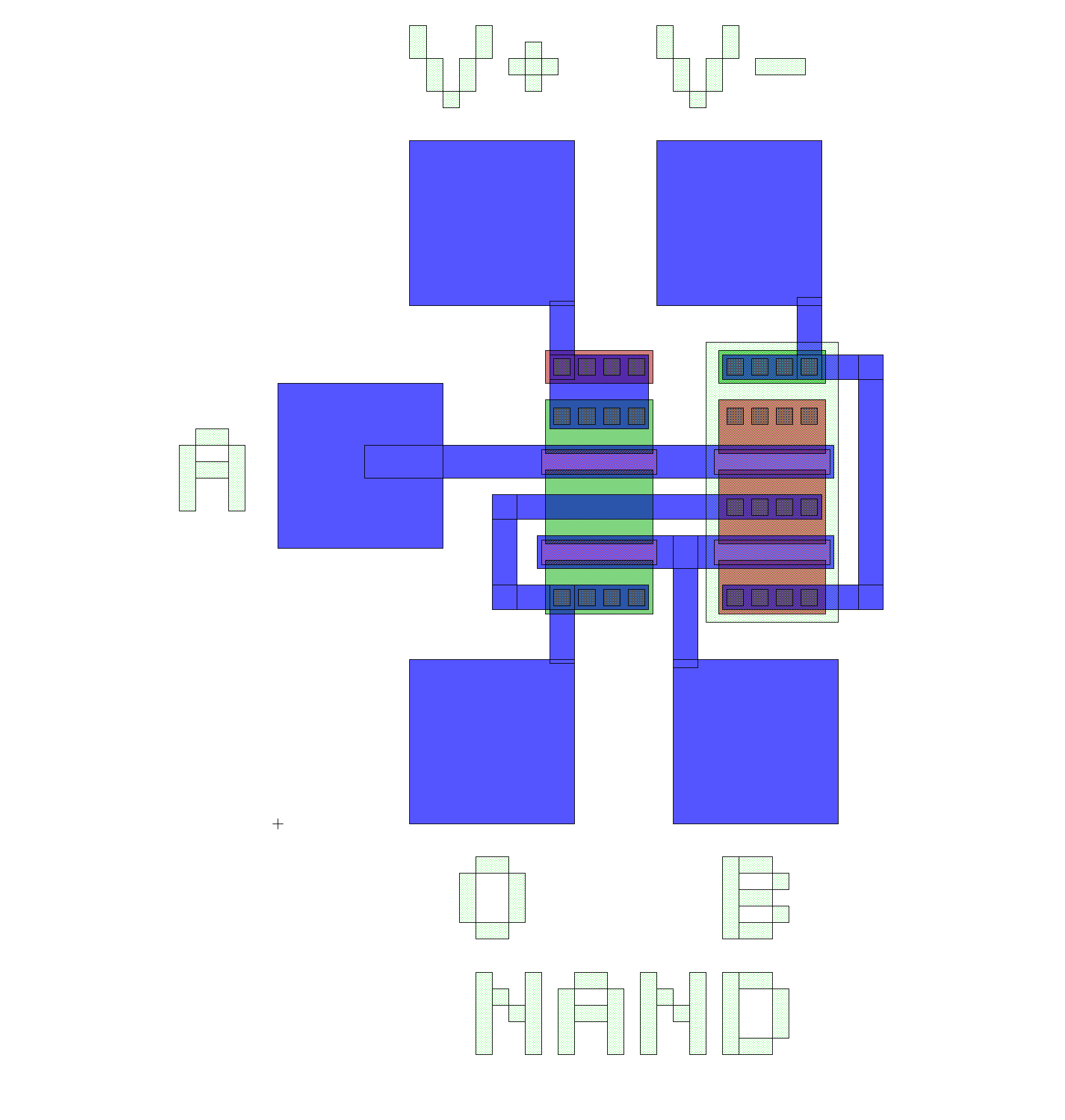
Layout of NAND gate
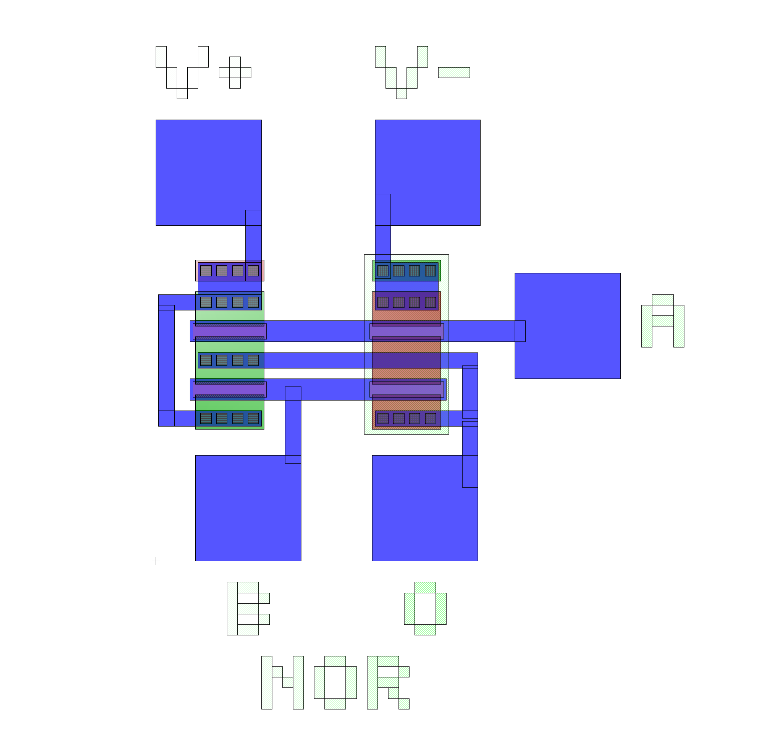
Layout of NOR
Layout of a BJT
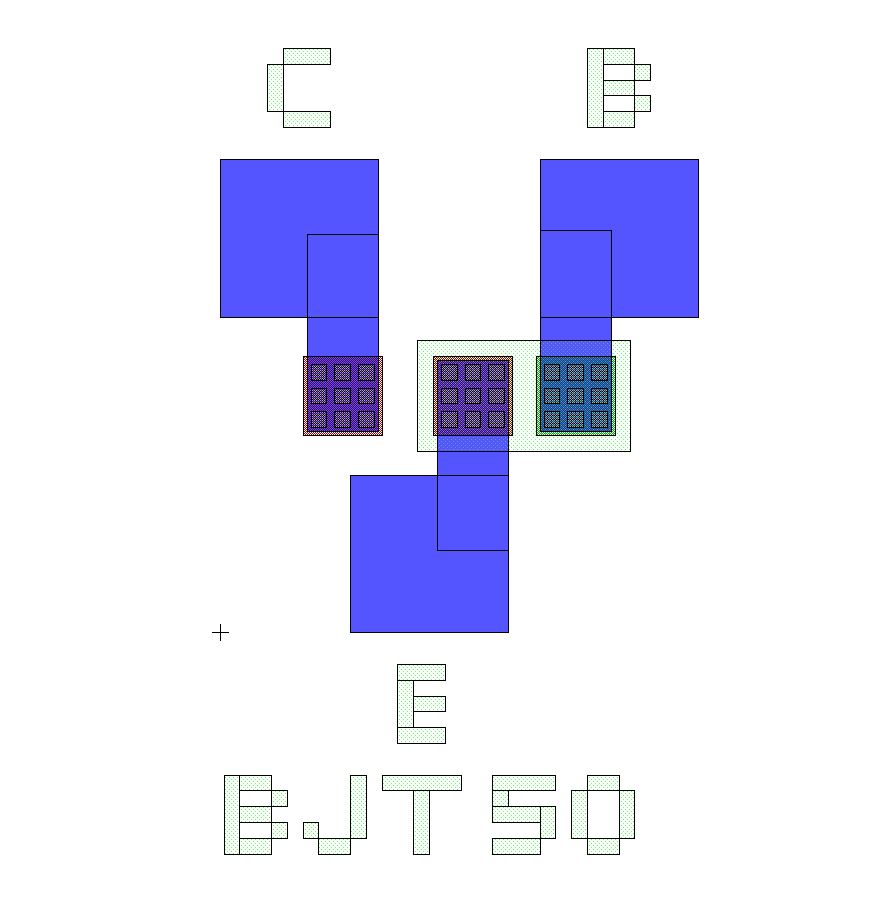
Layout of a single die